- 您现在的位置:买卖IC网 > Sheet目录2008 > MAX11602EEE+ (Maxim Integrated Products)IC ADC SERIAL 8BIT 8CH 16-QSOP
MAX11600–MAX11605
2.7V to 3.6V and 4.5V to 5.5V, Low-Power,
4-/8-/12-Channel 2-Wire Serial 8-Bit ADCs
20
______________________________________________________________________________________
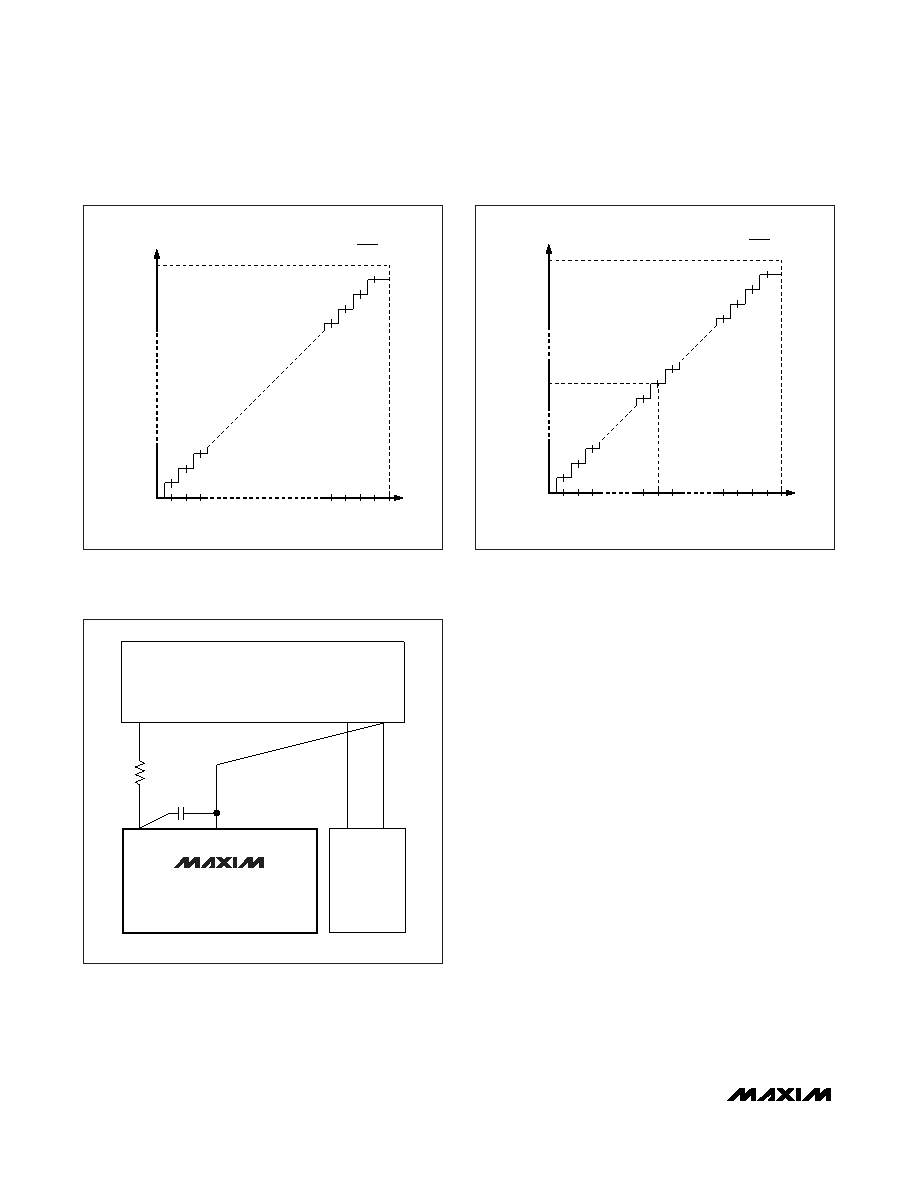
Layout, Grounding, and Bypassing
For best performance, use PC boards. Wire-wrap config-
urations are not recommended since the layout should
ensure proper separation of analog and digital traces. Do
not run analog and digital lines parallel to each other, and
do not lay out digital signal paths underneath the ADC
package. Use separate analog and digital PCB ground
sections with only one star point (Figure 14) connecting
the two ground systems (analog and digital). For lowest
noise operation, ensure the ground return to the star
ground’s power supply is low impedance and as short as
possible. Route digital signals far away from sensitive
analog and reference inputs.
High-frequency noise in the power supply (VDD) could
influence the proper operation of the ADC’s fast
comparator. Bypass VDD to the star ground with a
0.1F capacitor located as close as possible to the
MAX11600–MAX11605 power-supply pin. Minimize
capacitor lead length for best supply-noise rejection,
and add an attenuation resistor (5
) if the power sup-
ply is extremely noisy.
INPUT VOLTAGE (LSB)
OUTPUT CODE
1...111
1...110
1...101
1...100
0...000
0...001
0...010
0...011
23
256
VREF
1 LSB =
1
253
255
254
REF
256
0
252
Figure 12. Unipolar Transfer Function
INPUT VOLTAGE (LSB)
OUTPUT CODE
(TWO'S COMPLEMENT)
0...111
0...110
0...101
0...100
1...000
1...001
1...010
1...011
-1
-126 -125
256
VREF
1 LSB =
0+1
-127
+125
+127
+126
0...000
0...001
1...111
REF
+128
-128
+124
NEGATIVE INPUT
Figure 13. Bipolar Transfer Function
3V/5V
VLOGIC = 3V/5V
GND
SUPPLIES
DGND
3V/5V
GND
0.1
F
VDD
DIGITAL
CIRCUITRY
MAX11600–
MAX11605
R* = 5
*OPTIONAL
Figure 14. Power-Supply and Grounding Connections
发布紧急采购,3分钟左右您将得到回复。
相关PDF资料
MAX11610EEE+T
IC ADC SERIAL 10BIT 12CH 16-QSOP
MAX11616EEE+T
IC ADC SERIAL 12BIT 12CH 16-QSOP
MAX1162AEUB+T
IC ADC 16BIT 200KSPS 10-MSOP
MAX11637EEE+T
IC ADC 12BIT 8CH 16QSOP
MAX11643EEG+T
IC ADC 8BIT 8CH 24QSOP
MAX11645EUA+T
IC ADC 12BIT I2C/SRL 1CH 8UMAX
MAX11647EUA+T
IC ADC 10BIT I2C 94.4KSPS 8UMAX
MAX1166BEUP+
IC ADC 16BIT 165KSPS 20-TSSOP
相关代理商/技术参数
MAX11602EEE+T
功能描述:模数转换器 - ADC 8-Bit 8Ch 188ksps 5.5V Precision ADC RoHS:否 制造商:Texas Instruments 通道数量:2 结构:Sigma-Delta 转换速率:125 SPs to 8 KSPs 分辨率:24 bit 输入类型:Differential 信噪比:107 dB 接口类型:SPI 工作电源电压:1.7 V to 3.6 V, 2.7 V to 5.25 V 最大工作温度:+ 85 C 安装风格:SMD/SMT 封装 / 箱体:VQFN-32
MAX11603
制造商:MAXIM 制造商全称:Maxim Integrated Products 功能描述:2.7V to 3.6V and 4.5V to 5.5V, Low-Power, 4-/8-/12-Channel 2-Wire Serial 8-Bit ADCs
MAX11603EEE+
功能描述:模数转换器 - ADC 8-Bit 8Ch 188ksps 3.6V Precision ADC RoHS:否 制造商:Texas Instruments 通道数量:2 结构:Sigma-Delta 转换速率:125 SPs to 8 KSPs 分辨率:24 bit 输入类型:Differential 信噪比:107 dB 接口类型:SPI 工作电源电压:1.7 V to 3.6 V, 2.7 V to 5.25 V 最大工作温度:+ 85 C 安装风格:SMD/SMT 封装 / 箱体:VQFN-32
MAX11603EEE+T
功能描述:模数转换器 - ADC 8-Bit 8Ch 188ksps 3.6V Precision ADC RoHS:否 制造商:Texas Instruments 通道数量:2 结构:Sigma-Delta 转换速率:125 SPs to 8 KSPs 分辨率:24 bit 输入类型:Differential 信噪比:107 dB 接口类型:SPI 工作电源电压:1.7 V to 3.6 V, 2.7 V to 5.25 V 最大工作温度:+ 85 C 安装风格:SMD/SMT 封装 / 箱体:VQFN-32
MAX11604
制造商:MAXIM 制造商全称:Maxim Integrated Products 功能描述:2.7V to 3.6V and 4.5V to 5.5V, Low-Power, 4-/8-/12-Channel 2-Wire Serial 8-Bit ADCs
MAX11604EEE+
功能描述:模数转换器 - ADC 8-Bit 12Ch 188ksps 5.5V Precision ADC RoHS:否 制造商:Texas Instruments 通道数量:2 结构:Sigma-Delta 转换速率:125 SPs to 8 KSPs 分辨率:24 bit 输入类型:Differential 信噪比:107 dB 接口类型:SPI 工作电源电压:1.7 V to 3.6 V, 2.7 V to 5.25 V 最大工作温度:+ 85 C 安装风格:SMD/SMT 封装 / 箱体:VQFN-32
MAX11604EEE+T
功能描述:模数转换器 - ADC 8-Bit 12Ch 188ksps 5.5V Precision ADC RoHS:否 制造商:Texas Instruments 通道数量:2 结构:Sigma-Delta 转换速率:125 SPs to 8 KSPs 分辨率:24 bit 输入类型:Differential 信噪比:107 dB 接口类型:SPI 工作电源电压:1.7 V to 3.6 V, 2.7 V to 5.25 V 最大工作温度:+ 85 C 安装风格:SMD/SMT 封装 / 箱体:VQFN-32
MAX11605
制造商:MAXIM 制造商全称:Maxim Integrated Products 功能描述:2.7V to 3.6V and 4.5V to 5.5V, Low-Power, 4-/8-/12-Channel 2-Wire Serial 8-Bit ADCs